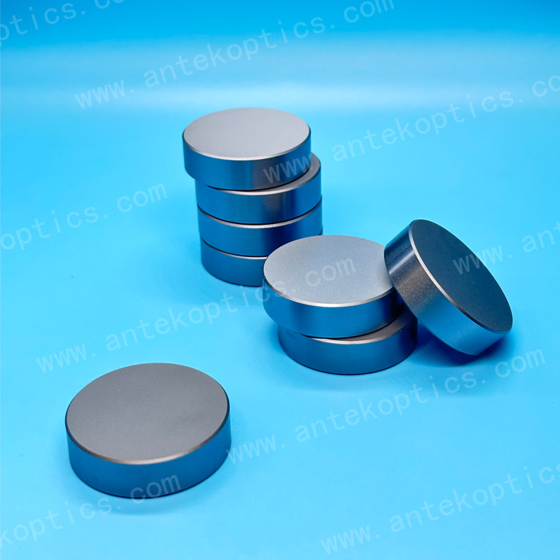
Custom wafer parameters
| Growth | CZ, FZ |
| Grade | Preme, test, Dummy, |
| Diameter | 1-12 inch/25.4-300mm |
| Thickness | 50~775um |
| Finish | As cut, lapped, etched, SSP, DSP, etc |
| Orientation | (100)(111)(110) |
| Off cut | up to 4 deg |
| Type/Dopant | P/B, N/Phos, N/As, N/Sb, Intrinsic |
| Resistivity | CZ:From 0.001 to 100 ohm-cm FZ:>3000 ohm-cm |
| Thin films | *PVD:AI,Cu,Au,Cr,Si,Ni,Fe,Mo.etc,Coating thicknesses up to 20,000Å/±5 *LPCVD/PECVD:OxIDE,Nitride,SiC,etc,Coating thicknesses up to 20,000Å/±3%% *Silicon epitaxial wafers and epitaxial services(SOS,GaN,GOI etc) |
| Processes | DSP,ultra thin,ultra flat,etc Downsizing,back grinding,dicing,etc. MEMS |
Other customizable wafers:
上一篇: Si3N4
下一篇: Silicon Warfer(FZ)